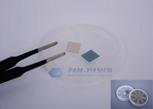
6H Semi-Insulating SiC Substrate With Cmp Polished, Research Grade,10mm x 10mm
PAM-XIAMEN offers semiconductor silicon carbide wafers,6H SiC and 4H SiC in different quality grades for researcher and industry manufacturers. We has developed SiC crystal growth technology and SiC crystal wafer processing technology,established a production line to manufacturer SiCsubstrate,Which is applied in GaNepitaxydevice,powerdevices,high-temperature device and optoelectronic Devices. As a professional company invested by the leading manufacturers from the fields of advanced and high-tech material research and state institutes and China’s Semiconductor Lab,weare devoted to continuously improve the quality of currently substrates and develop large size substrates.
Here shows detail specification:
SILICON CARBIDE MATERIAL PROPERTIES
| Polytype |
Single Crystal 4H |
Single Crystal 6H |
| Lattice Parameters |
a=3.076 Å |
a=3.073 Å |
| |
c=10.053 Å |
c=15.117 Å |
| Stacking Sequence |
ABCB |
ABCACB |
| Band-gap |
3.26 eV |
3.03 eV |
| Density |
3.21 · 103 kg/m3 |
3.21 · 103 kg/m3 |
| Therm. Expansion Coefficient |
4-5×10⁻⁶/K |
4-5×10⁻⁶/K |
| Refraction Index |
no = 2.719 |
no = 2.707 |
| |
ne = 2.777 |
ne = 2.755 |
| Dielectric Constant |
9.6 |
9.66 |
| Thermal Conductivity |
490 W/mK |
490 W/mK |
| Break-Down Electrical Field |
2-4 · 108 V/m |
2-4 · 108 V/m |
| Saturation Drift Velocity |
2.0 · 105 m/s |
2.0 · 105 m/s |
| Electron Mobility |
800 cm2/V·S |
400 cm2/V·S |
| hole Mobility |
115 cm2/V·S |
90 cm2/V·S |
| Mohs Hardness |
~9 |
~9 |
6H Semi-Insulating SiC Substrate, Research Grade,10mm x 10mm
| SUBSTRATE PROPERTY |
S6H-51-SI-PWAM-250 S6H-51-SI-PWAM-330 S6H-51-SI-PWAM-430 |
| Description |
Research Grade 6H SEMI Substrate |
| Polytype |
6H |
| Diameter |
(50.8 ± 0.38) mm |
| Thickness |
(250 ± 25) μm (330 ± 25) μm (430 ± 25) μm |
| Resistivity (RT) |
>1E5 Ω·cm |
| Surface Roughness |
< 0.5 nm (Si-face CMP Epi-ready); <1 nm (C- face Optical polish) |
| FWHM |
<50 arcsec |
| Micropipe Density |
A+≤1cm-2 A≤10cm-2 B≤30cm-2 C≤50cm-2 D≤100cm-2 |
| Surface Orientation |
| On axis <0001>± 0.5° |
| Off axis 3.5° toward <11-20>± 0.5° |
| Primary flat orientation |
Parallel {1-100} ± 5° |
| Primary flat length |
16.00 ± 1.70 mm |
| Secondary flat orientation Si-face:90° cw. from orientation flat ± 5° |
| C-face:90° ccw. from orientation flat ± 5° |
| Secondary flat length |
8.00 ± 1.70 mm |
| Surface Finish |
Single or double face polished |
| Packaging |
Single wafer box or multi wafer box |
| Usable area |
≥ 90 % |
| Edge exclusion |
1 mm |
SiC crystal application
Many researchers know the general SiCapplication:III-V Nitride Deposition;OptoelectronicDevices;High Power Devices;High Temperature Devices;High Frequency Power Devices.But few people knows detail applications, We list some detail application and make some explanations.
Detail Application of Silicon Carbide
Because of SiC physical and electronic properties,silicon carbide based device are well suitable for short wavelength optoelectronic, high temperature, radiation resistant, and high-power/high-frequency electronic devices,compared with Si and GaAs based device.
Many researchers know the general SiC application:III-V Nitride Deposition;Optoelectronic Devices;High Power Devices;High Temperature Devices;High Frequency Power Devices.But few people knows detail applications, here we list some detail application and make some explanations:
1. SiC substrate for X-ray monochromators:such as,using SiC's large d-spacing of about 15 A;
2. SiC substrate for high voltage devices;
3. SiC substrate for diamond film growth by microwave plasma-enhanced chemical vapor deposition;
4. For silicon carbide p-n diode;
5. SiC substrate for optical window: such as for very short (< 100 fs) and intense (> 100 GW/cm2) laser pulses with a wavelength of 1300 nm. It should have a low absorption coefficient and a low two photon absorption coefficient for 1300 nm.
6. SiC substrate for heat spreader: For example,the Silicon carbide crystal will be capillary bonded on a flat gain chip surface of VECSEL (Laser) to remove the generated pump heat. Therefore, the following properties are important:
1) Semi-insulating type required to prevent free carrier absorption of the laser light;
2) Double side polished are preferred;
3) Surface roughness: < 2nm, so that the surface is enough flat for bonding;
7. SiC substrate for THz system application: Normally it require THz transparency
8. SiC substrate for epitaxial graphene on SiC:Graphene epitaxy on off axis substrate and on axis are both available, surface side on C-face or Si face are both available.
9. SiC substrate for process development loke ginding, dicing and etc
10. SiC substrate for fast photo-electric switch
11. SiC substrate for heat sink: thermal conductivity and thermal expansion are concerned.
12. SiC substrate for laser: optical, surface and stranparence are concerned.
13. SiC substrate for III-V epitaxy, normally off axis substrate are required.
Xiamen Powerway Advanced Material Co.,Limited is an expert in SiC substrate, he can give researchers suggestions in different application
Saturation Velocity:
Saturation velocity is the maximum velocity a charge carrier in a semiconductor, generally an electron, attains in the presence of very high electric fields[1]. Charge carriersnormally move at an average drift speed proportional to the electric field strength they experience temporally. The proportionality constant is known as mobility of the carrier, which is a material property. A good conductor would have a high mobility value for its charge carrier, which means higher velocity, and consequently higher current values for a given electric field strength. There is a limit though to this process and at some high field value, a charge carrier can not move any faster, having reached its saturation velocity, due to mechanisms that eventually limit the movement of the carriers in the material.
When designing semiconductor devices, especially on a sub-micrometre scale as used in modern microprocessors, velocity saturation is an important design characteristic. Velocity saturation greatly affects the voltage transfer characteristics of a field-effect transistor, which is the basic device used in most integrated circuits designed and produced in the world. If a semiconductor device enters velocity saturation, an increase in voltage applied to the device will not cause a linear increase in current as would be expected by Ohm's law. Instead, the current may only increase by a small amount, or not at all. It is possible to take advantage of this result when trying to design a device that will pass a constant current regardless of the voltage applied, a current limiter in effect.
Product Tags:

|
|
6H Semi-Insulating SiC Substrate With Cmp Polished, Research Grade,10mm x 10mm Images
|