4 Inch Mg-Doped GaN Material On C(0001) Sapphire Substrates
PAM-XIAMEN’s Template Products consist of crystalline layers of gallium nitride (GaN), aluminum nitride (AlN),aluminum gallium nitride (AlGaN)and indium gallium nitride (InGaN), which are deposited on sapphire substrates. PAM-XIAMEN’s Template Products enable 20-50% shorter epitaxy cycle times and higher quality epitaxial device layers, with better structural quality and higher thermal conductivity,which can improve devices in the cost, yield, and performance.
PAM-XIAMEN’sGaN on sapphire templates are available in diameters from 2" up to 6",and consist of a thin layer of crystalline GaN grown on a sapphire substrate. Epi-ready templates now available..
Here shows detail specification:
4inch Mg-Doped GaN/Sapphire Substrates
| Item | PAM-T-GaN-100-P |
| Dimension | 100 ±0.1 mm |
| Thickness | 5 ±1 μm |
| Orientation of GaN | C plane (0001) off angle toward A-axis 0.2 ±0.1° |
| Orientation Flat of GaN | (1-100) 0 ±0.2°, 16 ±1 mm |
| Conduction Type | P-type |
| Resistivity (300K) | ~ 10 Ω·cm |
| Carrier Concentration | >6X10¹⁶CM-3(doping concentration≥10x1020cm-3 |
| Mobility | ~ 10cm2 / V·s |
| Dislocation Density | < 5x108cm-2(estimated by FWHMs of XRD) |
| Structure | 2~2.5 μm pGaN/2~2.5 μm pGaN uGaN/50nm uGaN buffer layer/430±25μm |
| Orientation of Sapphire | C plane (0001) off angle toward M-axis 0.2 ±0.1° |
| Orientation Flat of Sapphire | (11-20) 0 ±0.2°, 16 ±1 mm |
| Surface Roughness: | Front side: Ra<0.5nm, epi-ready;
Back side: etched or polished. |
| Useable Area | > 90% (edge and macro defects exclusion) |
| Package | each in single wafer container, under nitrogen atmosphere, packed in class 100 clean room |
4inch Mg-Doped GaN/Sapphire Substrates
FWHM and XRD report
A test report is necessary to show the compliance between custom description and our final wafers data. We will test the wafer characerization by equipment before shipment, testing surface roughness by atomic force microscope, type by Roman spectra instrument, resistivity by non-contact resistivity testing equipment,micropipe density by polarizing microscope, orientation by X-ray Orientator etc. if the wafers meet the requirement, we will clean and pack them in 100 class clean room, if the wafers do not match the custom spec, we will take it off.
Testing Project: FWHM and XRD project
The half-height full width (FWHM) is an expression of the range of functions given by the difference between two extreme values of the independent variable equal to half of its maximum. In other words, it is the width of the spectral curve measured between those points on the Y-axis, which is half the maximum amplitude.
Below is an example of FWHM and XRD of AlN template:
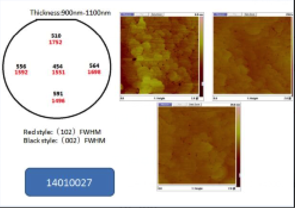
FWHM and XRD of AlN template
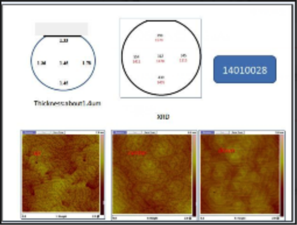
FWHM and XRD of AlN template
Here we show experiment as an example:
Experiment on GaN on sapphire:Optoelectronic Properties and Structural Characterization of GaN Thick Films on Different Substrates through Pulsed Laser Deposition:
Experiment on GaN on sapphire:Optoelectronic Properties and Structural Characterization of GaN Thick Films on Different Substrates through Pulsed Laser Deposition:
All GaN film samples were deposited on different substrates by PLD at 1000 ◦C in a nitrogen plasma ambient atmosphere. The chamber was pumped down to 10−6 Torr before the deposition process began, and N2 gas (with a purity of 99.999%) was introduced. The working pressure once the N2 plasma was injected was 1.13 × 10⁻⁴ Torr. A KrF excimer laser (λ = 248 nm, Lambda Physik, Fort Lauderdale, FL, USA) was employed as the ablation source and operated with a repetition rate of 1 Hz and a pulse energy of 60 mJ. The average growth rate of the GaN film was approximately 1 µm/h. The laser beam was incident on a rotating target at an angle of 45◦ . The GaN target was fabricated by HVPE and set at a fixed distance of 9 cm from the substrate before being rotated at 30 rpm during film deposition. In this case, ~4 µm-thick GaN films were grown on a GaN/sapphire template (sample A), sapphire (sample B), Si(111) (sample C), and Si(100) (sample D). For the GaN on sample A, a 2-µm GaN layer was firstly deposited on sapphire substrate by MOCVD. Scanning electron microscopy (SEM, S-3000H, Hitachi, Tokyo, Japan), transmission electron microcopy (TEM, H-600, Hitachi, Tokyo, Japan), atomic force microscopy (AFM, DI-3100, Veeco, New York, NY, USA), double-crystal X-ray diffraction (XRD, X’Pert PRO MRD, PANalytical, Almelo, The Netherlands), low-temperature photoluminescence (PL, Flouromax-3, Horiba, Tokyo, Japan), and Raman spectroscopy (Jobin Yvon, Horiba, Tokyo, Japan) were employed to explore the microstructure and optical properties of the GaN templates deposited on different substrates. The electrical properties of the GaN films were determined by Van der Pauw-Hall measurement under liquid nitrogen cooling at 77 K
N/sapphire template and sapphire. The calculated values of stress for GaN grown on different substrates are shown in Figure 7. The Raman spectra of the MGS sample is displayed for comparison, as shown in Figure 7. The GaN E2 peak of MGS was evaluated at 570.2 cm−1 with a compressive stress value of −0.548 GPa, which is larger than the compressive stress value of −0.468 for sample B. It can be concluded that the PLD growth method is beneficia for the release of stress in the films.
Cross-sectional TEM images were used to investigate the GaN-on-Si meltback-etching reaction with PLD operating at a high temperature of 1000 ◦C. Previously, it was reported that the meltback-etching process caused by alloying reaction Ga with Si leads to a rough GaN surface and deep hollows in the Si substrate [39,40].
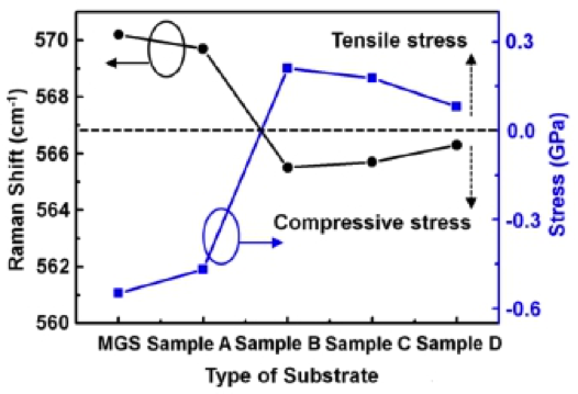
Figure 7. Residual stress and its corresponding E2 Raman shift for samples MGS, A, B, C, and D.
Product Tags:

|
|
4 Inch Mg-Doped GaN Material On C(0001) Sapphire Substrates Images
|