N Type ,InAs(Indium Arsenide ) Wafer , 2”, Mechanical Grade
PAM-XIAMEN provides single crystal InAs(Indium arsenide) wafer for infrared detectors, photovoltaic photodiodes detectors, diode lasers in lower noise or higher-power applications at room temperature. in diameter up to 4 inch. Indium Arsenide ( InAs ) crystal is formed by two elements , Indium and Arsenide , growth by Liquid Encapsulated Czochralski ( LEC ) method or VGF method . InAs wafer is is similar to gallium arsenide and is a direct bandgap material.
Indium arsenide is sometimes used together with indium phosphide. Alloyed with gallium arsenide it forms indium gallium arsenide - a material with band gap dependent on In/Ga ratio, a method principally similar to alloying indium nitride with gallium nitride to yield indium gallium nitride. PAM-XIAMEN can provide epi ready grade InAs wafer for your MOCVD & MBE epitaxial application .Please contact our engineer team for more wafer information.
2" InAs Wafer Specification
| Item | Specifications |
| Dopant | Stannum | Sulphur |
| Conduction Type | N-type | N-type |
| Wafer Diameter | 2" |
| Wafer Orientation | (100)±0.5° |
| Wafer Thickness | 500±25um |
| Primary Flat Length | 16±2mm |
| Secondary Flat Length | 8±1mm |
| Carrier Concentration | (5-20)x1017cm-3 | (1-10)x1017cm-3 |
| Mobility | 7000-20000cm2/V.s | 6000-20000cm2/V.s |
| EPD | | <5x104cm-2 | <3x104cm-2 |
| TTV | <10um |
| BOW | <10um |
| WARP | <12um |
| Laser marking | upon request |
| Suface finish | P/E, P/P |
| Epi ready | yes |
| Package | Single wafer container or cassette |
What is a InAs test Wafer?
Most test wafers are wafers which have fallen out of prime specifications. Test wafers may be used to run marathons, test equipment and for high-end R & D. They are often a cost-effective alternative to prime wafers.
Band structure and carrier concentration of InAs Wafer
Basic Parameters
| Energy gap | 0.354 eV |
| Energy separation (EΓL) between Γ and L valleys | 0.73 eV |
| Energy separation (EΓX) between Γ and X valleys | 1.02 eV |
| Energy spin-orbital splitting | 0.41 eV |
| Intrinsic carrier concentration | 1·1015 cm-3 |
| Intrinsic resistivity | 0.16 Ω·cm |
| Effective conduction band density of states | 8.7·1016 cm-3 |
| Effective valence band density of states | 6.6·1018 cm-3 |
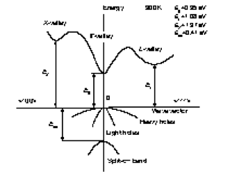 | Band structure and carrier concentration of InAs.
Important minima of the conduction band and maxima of the valence band.
Eg= 0.35 eV
EL= 1.08 eV
EX= 1.37 eV
Eso = 0.41 eV |
Temperature Dependences
Temperature dependence of the direct energy gap
Eg = 0.415 - 2.76·10-4·T2/(T+83) (eV),
where T is temperature in degrees K (0 <T < 300).
Effective density of states in the conduction band
Nc≈1.68·1013·T3/2 (cm-3).
Effective density of states in the valence band
Nv≈ 1.27·1015·T3/2(cm-3).
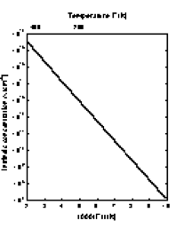 | The temperature dependences of the intrinsic carrier concentration. |
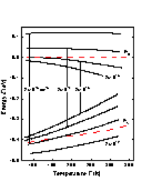 | Fermi level versus temperature for different concentrations of shallow donors and acceptors. |
Dependences on Hydrostatic Pressure
Eg≈Eg(0) + 4.8·10-3P (eV)
EL≈ EL(0) + 3.2·10-3P (eV)
where P is pressure in kbar
Energy Gap Narrowing at High Doping Levels
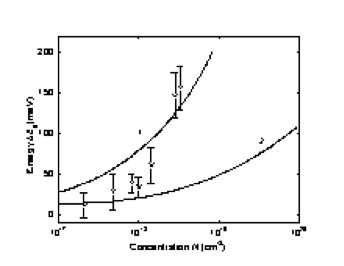 | Energy gap narrowing versus donor (Curve 1) and acceptor (Curve 2 ) doping density.
Curves are calculated according
Points show experimental results for n-InAs |
For n-type InAs
ΔEg = 14.0·10-9·Nd1/3 + 1.97·10-7·Nd1/4 + 57.9·10-12·Nd1/2 (eV)
For p-type InAs
ΔEg = 8.34·10-9·Na1/3 + 2.91·10-7·Na1/4 + 4.53·10-12·Na1/2 (eV)
Effective Masses
Electrons:
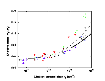 | Electron effective mass versus electron concentration
|
| For Γ-valley | mΓ = 0.023mo |
Nonparabolicity:
E(1+αE) = h2k2/(2mΓ) | α = 1.4 (eV-1) |
| In the L-valley effective mass of density of states | mL=0.29mo |
| In the X-valley effective mass of density of states | mX=0.64mo |
Holes:
| Heavy | mh = 0.41mo |
| Light | mlp = 0.026mo |
| Split-off band | mso = 0.16mo |
Effective mass of density of states mv = 0.41mo
Donors and Acceptors
Ionization energies of shallow donors
≥ 0.001(eV): Se, S, Te, Ge, Si, Sn, Cu
Ionization energies of shallow acceptors, eV
| Sn | Ge | Si | Cd | Zn |
| 0.01 | 0.014 | 0.02 | 0.015 | 0.01 |
Are You Looking for an InAs substrate?
PAM-XIAMEN is proud to offer indium phosphide substrate for all different kinds of projects. If you are looking for InAs wafers, send us enquiry today to learn more about how we can work with you to get you the InAs wafers you need for your next project. Our group team is looking forward to providing both quality products and excellent service for you!
Product Tags:

|
|
N Type ,InAs(Indium Arsenide ) Wafer , 2”, Mechanical Grade Images
|

